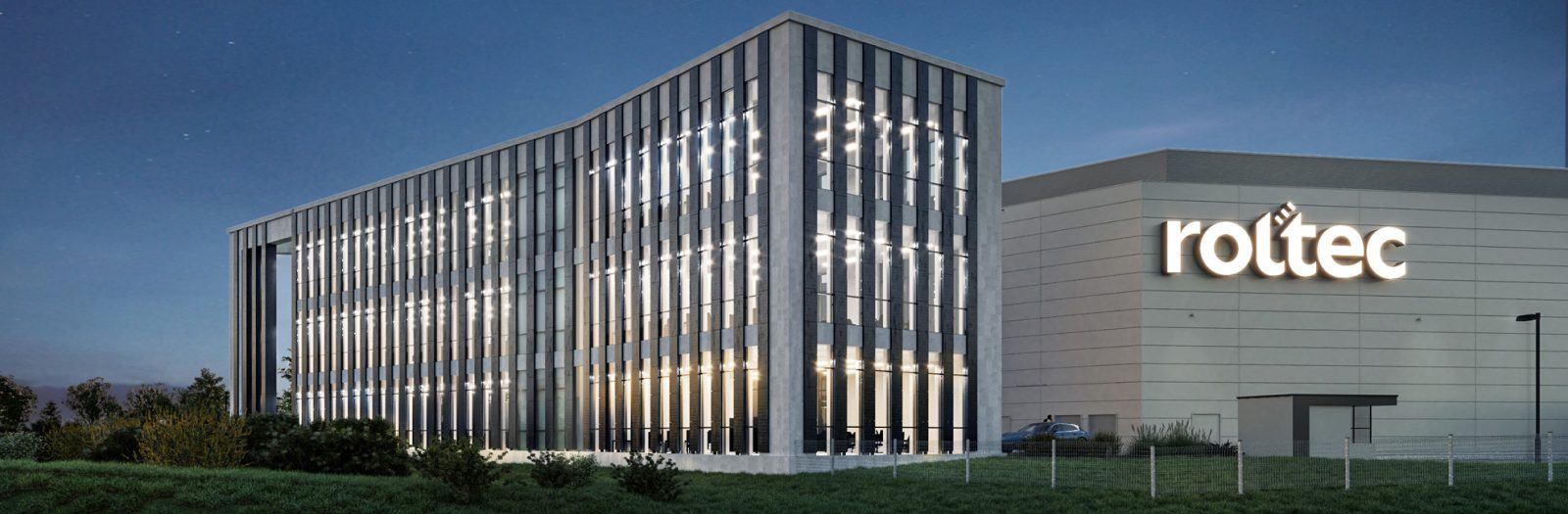
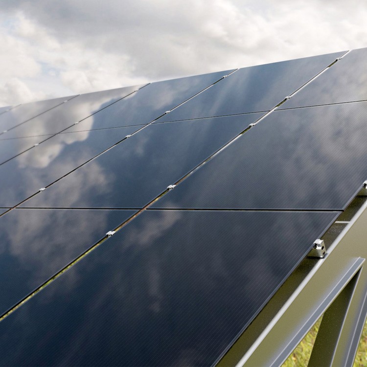
CIGS panel factory
Roltec plans to launch the first thin-film photovoltaic cell factory in Poland in CIGS technology in 2023. Technology Readiness Level at Roltec allowed for the development of large-scale production of CIGS modules, while maintaining the highest standards of quality and repeatability.
High-efficiency photovoltaic panels manufactured in the Wrocław factory will be our answer to the growing demand of the renewable energy market. We wish to pursue our Mission to create a more sustainable future. We believe that our business and investment strategy will fit into the framework of the UN and EU Sustainable Development Policy, and will remain the permanent basis of our approach to development and operational practices.
The German technology (Solibro GmbH) acquired by, implemented and constantly improved at Roltec allows the commercialization of a revolutionary product that will have a significant advantage in every aspect (price, speed and ease of installation, performance, warranty, aesthetics) over silicon cells.
The aesthetic, frameless Solvoz panels will ensure energy production in all lighting conditions, while guaranteeing a 15% higher yield * per installed kWp.
* compared to silicon panels

Project in numbers:
CIGS technology

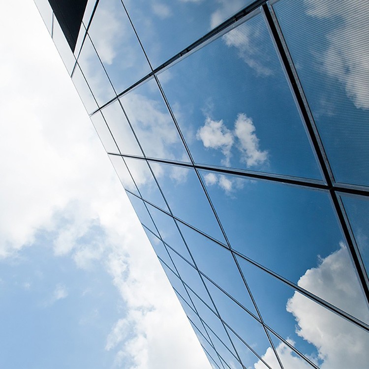
Durability, effective work and aesthetics make CIGS conquer construction market. Thin-film PV technologies in practice make use of photovoltaics in urban space and landscape architecture (facade panels), creating ecological integrated solutions BIPV (Building-Integrated Photovoltaics) and BAPV (Building-Attached Photovoltaics).

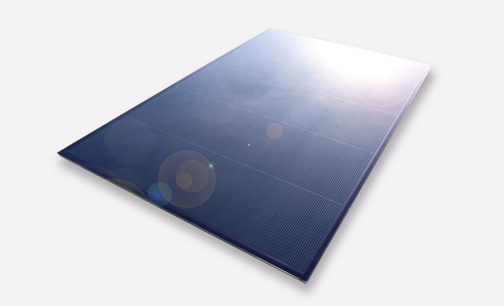
Due to the high absorption of even low light and a low temperature coefficient, CIGS panels are characterized by high efficiency even in difficult conditions. Non-toxic and safe cells are 98% recyclable. Solvoz panels will be used primarily in large-scale energy production for the needs of enterprises (photovoltaic farms).

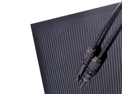
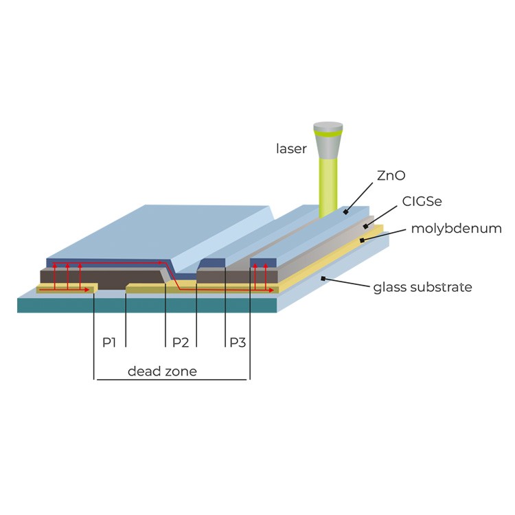
Copper Indium Gallium and Selenide, or CIGS, is a technology of thin solar cells (photovoltaic) based on the deposition of four elements (copper, indium, gallium, selenium) on any substrate. It is distinguished from many other technologies by the best spectral response, i.e. radiation absorption. The great advantage of our technology is its high efficiency with the use of a small amount of material.